• Global Semiconductor Inspection Equipment Market Valued at USD 8.88 Billion in 2024, Set for Strong Growth Through 2032
    The global Semiconductor Inspection Equipment Market, valued at USD 8,879 million in 2024, is poised for steady growth, projected to increase from USD 9,320 million in 2025 to USD 12,380 million by 2032. This represents a compound annual growth rate (CAGR) of 5.0% during the forecast period, according to a comprehensive new analysis by Semiconductor Insight. The report underscores the indispensable role of inspection and metrology systems in maintaining the integrity and yield of semiconductor manufacturing, a sector where nanometer-scale defects can lead to catastrophic financial losses.
    Semiconductor inspection equipment, crucial for identifying defects and measuring critical dimensions during chip fabrication, has become a cornerstone of modern electronics production. As transistor densities increase and geometries shrink below 5 nanometers, the need for sophisticated inspection technologies capable of detecting sub-nanometer imperfections has intensified, making these systems vital for maintaining high yields in advanced manufacturing processes. The equipment's ability to provide real-time process control and rapid feedback loops allows manufacturers to quickly identify and correct process deviations, significantly reducing scrap and improving overall operational efficiency.
    Strategic Imperative: The Critical Role of Inspection in Semiconductor Manufacturing
    The relentless advancement of semiconductor technology serves as the primary catalyst for inspection equipment demand. As the industry transitions to more complex 3D architectures like gate-all-around transistors and advanced packaging schemes such as chiplets, the inspection challenges multiply exponentially. This technological evolution directly correlates with increased inspection intensity throughout the fabrication process. With semiconductor manufacturing involving up to 600 process steps for advanced nodes, the probability of defects increases substantially, making comprehensive inspection protocols not just beneficial but absolutely essential for economic viability.
    "The transition to advanced nodes below 7nm has fundamentally altered the inspection landscape," the report emphasizes. "Where optical inspection once sufficed, manufacturers now require hybrid systems combining multiple technologies to detect defects that were previously undetectable. The Asia-Pacific region, housing over 75% of global semiconductor manufacturing capacity, represents the most significant market for inspection equipment, with leading foundries and memory manufacturers continuously upgrading their inspection capabilities to maintain competitive yields." The push toward angstrom-level manufacturing at 2nm and beyond is creating unprecedented demand for inspection systems with atomic-scale resolution.
    Read Full Report: https://semiconductorinsight.com/report/semiconductor-inspection-equipment-market/

    ##SemiconductorIndustry,
    #Semiconductors,
    #ChipManufacturing,
    #Microelectronics,
    #ChipDesign,
    #WaferFabrication,
    #SemiconductorMarket,
    #AdvancedPackaging,
    #Nanotechnology,
    #AIChips
    , #PowerSemiconductors,
    #IntegratedCircuits,
    #Fabless, #Foundry,
    #ChipSupplyChain,
    #ElectronicsIndustry,
    #TechInnovation,
    #Photonics,
    #5GChips,
    #GlobalSemiconductors
    Global Semiconductor Inspection Equipment Market Valued at USD 8.88 Billion in 2024, Set for Strong Growth Through 2032 The global Semiconductor Inspection Equipment Market, valued at USD 8,879 million in 2024, is poised for steady growth, projected to increase from USD 9,320 million in 2025 to USD 12,380 million by 2032. This represents a compound annual growth rate (CAGR) of 5.0% during the forecast period, according to a comprehensive new analysis by Semiconductor Insight. The report underscores the indispensable role of inspection and metrology systems in maintaining the integrity and yield of semiconductor manufacturing, a sector where nanometer-scale defects can lead to catastrophic financial losses. Semiconductor inspection equipment, crucial for identifying defects and measuring critical dimensions during chip fabrication, has become a cornerstone of modern electronics production. As transistor densities increase and geometries shrink below 5 nanometers, the need for sophisticated inspection technologies capable of detecting sub-nanometer imperfections has intensified, making these systems vital for maintaining high yields in advanced manufacturing processes. The equipment's ability to provide real-time process control and rapid feedback loops allows manufacturers to quickly identify and correct process deviations, significantly reducing scrap and improving overall operational efficiency. Strategic Imperative: The Critical Role of Inspection in Semiconductor Manufacturing The relentless advancement of semiconductor technology serves as the primary catalyst for inspection equipment demand. As the industry transitions to more complex 3D architectures like gate-all-around transistors and advanced packaging schemes such as chiplets, the inspection challenges multiply exponentially. This technological evolution directly correlates with increased inspection intensity throughout the fabrication process. With semiconductor manufacturing involving up to 600 process steps for advanced nodes, the probability of defects increases substantially, making comprehensive inspection protocols not just beneficial but absolutely essential for economic viability. "The transition to advanced nodes below 7nm has fundamentally altered the inspection landscape," the report emphasizes. "Where optical inspection once sufficed, manufacturers now require hybrid systems combining multiple technologies to detect defects that were previously undetectable. The Asia-Pacific region, housing over 75% of global semiconductor manufacturing capacity, represents the most significant market for inspection equipment, with leading foundries and memory manufacturers continuously upgrading their inspection capabilities to maintain competitive yields." The push toward angstrom-level manufacturing at 2nm and beyond is creating unprecedented demand for inspection systems with atomic-scale resolution. Read Full Report: https://semiconductorinsight.com/report/semiconductor-inspection-equipment-market/ ##SemiconductorIndustry, #Semiconductors, #ChipManufacturing, #Microelectronics, #ChipDesign, #WaferFabrication, #SemiconductorMarket, #AdvancedPackaging, #Nanotechnology, #AIChips , #PowerSemiconductors, #IntegratedCircuits, #Fabless, #Foundry, #ChipSupplyChain, #ElectronicsIndustry, #TechInnovation, #Photonics, #5GChips, #GlobalSemiconductors
    Semiconductor Inspection Equipment Market, Global Business Strategies 2025-2032
    Semiconductor Inspection Equipment Market, Global Business Strategies 2025-2032
    semiconductorinsight.com
    Semiconductor Inspection Equipment Market size was valued at USD 9,320 million in 2025 to USD 12,380 million by 2032, exhibiting a CAGR of 5.0%
    0 留言 ·0 分享 ·279 瀏覽次數 ·0 評論
  • The global Semiconductor Inspection Equipment Market, valued at USD 8,879 million in 2024, is poised for steady growth, projected to increase from USD 9,320 million in 2025 to USD 12,380 million by 2032. This represents a compound annual growth rate (CAGR) of 5.0% during the forecast period, according to a comprehensive new analysis by Semiconductor Insight. The report underscores the indispensable role of inspection and metrology systems in maintaining the integrity and yield of semiconductor manufacturing, a sector where nanometer-scale defects can lead to catastrophic financial losses.
    Semiconductor inspection equipment, crucial for identifying defects and measuring critical dimensions during chip fabrication, has become a cornerstone of modern electronics production. As transistor densities increase and geometries shrink below 5 nanometers, the need for sophisticated inspection technologies capable of detecting sub-nanometer imperfections has intensified, making these systems vital for maintaining high yields in advanced manufacturing processes. The equipment's ability to provide real-time process control and rapid feedback loops allows manufacturers to quickly identify and correct process deviations, significantly reducing scrap and improving overall operational efficiency.
    Strategic Imperative: The Critical Role of Inspection in Semiconductor Manufacturing
    The relentless advancement of semiconductor technology serves as the primary catalyst for inspection equipment demand. As the industry transitions to more complex 3D architectures like gate-all-around transistors and advanced packaging schemes such as chiplets, the inspection challenges multiply exponentially. This technological evolution directly correlates with increased inspection intensity throughout the fabrication process. With semiconductor manufacturing involving up to 600 process steps for advanced nodes, the probability of defects increases substantially, making comprehensive inspection protocols not just beneficial but absolutely essential for economic viability.
    "The transition to advanced nodes below 7nm has fundamentally altered the inspection landscape," the report emphasizes. "Where optical inspection once sufficed, manufacturers now require hybrid systems combining multiple technologies to detect defects that were previously undetectable. The Asia-Pacific region, housing over 75% of global semiconductor manufacturing capacity, represents the most significant market for inspection equipment, with leading foundries and memory manufacturers continuously upgrading their inspection capabilities to maintain competitive yields." The push toward angstrom-level manufacturing at 2nm and beyond is creating unprecedented demand for inspection systems with atomic-scale resolution.
    Read Full Report: https://semiconductorinsight.com/report/semiconductor-inspection-equipment-market/
    ##SemiconductorIndustry,
    #Semiconductors,
    #ChipManufacturing,
    #Microelectronics,
    #ChipDesign,
    #WaferFabrication,
    #SemiconductorMarket,
    #AdvancedPackaging,
    #Nanotechnology,
    #AIChips
    The global Semiconductor Inspection Equipment Market, valued at USD 8,879 million in 2024, is poised for steady growth, projected to increase from USD 9,320 million in 2025 to USD 12,380 million by 2032. This represents a compound annual growth rate (CAGR) of 5.0% during the forecast period, according to a comprehensive new analysis by Semiconductor Insight. The report underscores the indispensable role of inspection and metrology systems in maintaining the integrity and yield of semiconductor manufacturing, a sector where nanometer-scale defects can lead to catastrophic financial losses. Semiconductor inspection equipment, crucial for identifying defects and measuring critical dimensions during chip fabrication, has become a cornerstone of modern electronics production. As transistor densities increase and geometries shrink below 5 nanometers, the need for sophisticated inspection technologies capable of detecting sub-nanometer imperfections has intensified, making these systems vital for maintaining high yields in advanced manufacturing processes. The equipment's ability to provide real-time process control and rapid feedback loops allows manufacturers to quickly identify and correct process deviations, significantly reducing scrap and improving overall operational efficiency. Strategic Imperative: The Critical Role of Inspection in Semiconductor Manufacturing The relentless advancement of semiconductor technology serves as the primary catalyst for inspection equipment demand. As the industry transitions to more complex 3D architectures like gate-all-around transistors and advanced packaging schemes such as chiplets, the inspection challenges multiply exponentially. This technological evolution directly correlates with increased inspection intensity throughout the fabrication process. With semiconductor manufacturing involving up to 600 process steps for advanced nodes, the probability of defects increases substantially, making comprehensive inspection protocols not just beneficial but absolutely essential for economic viability. "The transition to advanced nodes below 7nm has fundamentally altered the inspection landscape," the report emphasizes. "Where optical inspection once sufficed, manufacturers now require hybrid systems combining multiple technologies to detect defects that were previously undetectable. The Asia-Pacific region, housing over 75% of global semiconductor manufacturing capacity, represents the most significant market for inspection equipment, with leading foundries and memory manufacturers continuously upgrading their inspection capabilities to maintain competitive yields." The push toward angstrom-level manufacturing at 2nm and beyond is creating unprecedented demand for inspection systems with atomic-scale resolution. Read Full Report: https://semiconductorinsight.com/report/semiconductor-inspection-equipment-market/ ##SemiconductorIndustry, #Semiconductors, #ChipManufacturing, #Microelectronics, #ChipDesign, #WaferFabrication, #SemiconductorMarket, #AdvancedPackaging, #Nanotechnology, #AIChips
    Semiconductor Inspection Equipment Market, Global Business Strategies 2025-2032
    Semiconductor Inspection Equipment Market, Global Business Strategies 2025-2032
    semiconductorinsight.com
    Semiconductor Inspection Equipment Market size was valued at USD 9,320 million in 2025 to USD 12,380 million by 2032, exhibiting a CAGR of 5.0%
    0 留言 ·0 分享 ·150 瀏覽次數 ·0 評論
  • Global APD Avalanche Photodiode Market Valued

    The global APD Avalanche Photodiode Market was valued at USD 138 million in 2024. The market is projected to grow from USD 143 million in 2025 to USD 179 million by 2032, exhibiting a CAGR of 3.9% during the forecast period, according to a comprehensive new report published by Semiconductor Insight. This growth trajectory highlights the expanding role of APDs as critical components in systems requiring highly sensitive light detection, particularly in fields like autonomous driving, telecommunications, and medical imaging.
    Avalanche Photodiodes (APDs) are semiconductor devices that leverage the avalanche multiplication effect to detect low-intensity light signals with exceptional sensitivity and speed. This unique capability makes them indispensable in applications where traditional photodetectors fall short, such as long-range LiDAR, high-speed optical communication networks, and precision medical diagnostics. Their function in converting light into electrical signals with internal gain allows systems to operate effectively even in challenging low-light conditions, positioning APDs as foundational technology for numerous advanced systems.

    Download FREE Sample Report:
    APD Avalanche Photodiode Market - View in Detailed Research Report
    Automotive and LiDAR Expansion: The Primary Growth Engine
    The report identifies the rapid advancement and adoption of Automotive LiDAR as the paramount driver for the APD market's growth. The proliferation of autonomous vehicles and advanced driver-assistance systems (ADAS) is creating robust demand for high-sensitivity LiDAR systems that rely on APDs for accurate object detection and ranging. This segment's demand is propelled by the rapid integration of LiDAR technology into next-generation vehicles for enhanced autonomy and safety features. High-volume production requirements and stringent quality standards from automotive companies drive innovation and economies of scale in APD manufacturing.
    "The strategic focus on developing next-generation LiDAR systems for automotive safety and smart manufacturing applications continues to propel the demand for high-performance avalanche photodiodes," the report states. Collaborations between APD suppliers and automotive leaders are crucial for developing customized solutions that meet the demanding performance and reliability specifications of the automotive industry. The transition towards higher levels of vehicle autonomy, which requires more sophisticated and reliable sensing capabilities, further intensifies this trend.
    Read Full Report: https://semiconductorinsight.com/report/apd-avalanche-photodiode-market/
    Market Segmentation: Si APD and Automotive Applications Driving Dominance
    The report provides a detailed segmentation analysis, offering a clear view of the market structure and key growth segments:
    Segment Analysis:
    By Type
    • Si APD
    • InGaAs APD
    • Others
    By Application
    • Industrial
    • Medical
    • Mobility
    • Others
    By End User
    • Automotive OEMs & Tier-1 Suppliers
    • Telecommunication Service Providers
    • Medical Device Manufacturers
    • Industrial Equipment Manufacturers
    Download Sample Report: https://semiconductorinsight.com/download-sample-report/?product_id=127114
    Competitive Landscape: Key Players and Strategic Focus
    The global APD Avalanche Photodiode market is moderately concentrated, with the top three manufacturers collectively holding over 45% of the market share. Hamamatsu Photonics K.K. and First Sensor AG are recognized as global leaders, leveraging their extensive R&D capabilities and established semiconductor manufacturing expertise to dominate the high-performance segment. Their products are critical in applications requiring extreme sensitivity, such as LiDAR for autonomous vehicles and high-speed optical communication systems.
    The report profiles key industry players, including:
    • Hamamatsu Photonics K.K. (Japan)
    • First Sensor AG (Germany)
    • Kyosemi Corporation (Japan)
    • Luna Optoelectronics (U.S.)
    • Excelitas Technologies Corp. (U.S.)
    • Edmund Optics (U.S.)
    • GCS (China)
    • Accelink Technologies Co., Ltd. (China)
    • NORINCO GROUP (China)
    • LD-PD Inc. (U.S.)
    • Voxtel, Inc. (U.S.)
    • Laser Components GmbH (Germany)
    • Albis Optoelectronics AG (Switzerland)
    These companies are intensely focused on technological differentiation and material science innovation to enhance performance metrics such as quantum efficiency and noise characteristics. Many are also pursuing geographic expansion into high-growth regions to capture emerging opportunities, particularly in the Asia-Pacific market where manufacturing capabilities are rapidly scaling.
    Emerging Opportunities in Quantum Technology and Advanced Communications
    While automotive LiDAR represents the current growth frontier, the report outlines significant emerging opportunities in quantum technology and next-generation communications. The development of quantum computing and quantum key distribution (QKD) systems requires photodetectors with single-photon sensitivity, a domain where specialized APDs excel. Furthermore, the ongoing global expansion of fiber-optic communication infrastructure, including the push for higher bandwidth 5G and eventual 6G networks, creates sustained demand for high-speed APDs in optical receivers. The integration of APDs into new industrial automation and safety systems further expands their application horizon, underscoring their versatility beyond traditional markets.
    Report Scope and Availability
    The market research report offers a comprehensive analysis of the global and regional APD Avalanche Photodiode markets from 2025-2032. It provides detailed segmentation, market size forecasts, competitive intelligence, technology trends, and an evaluation of key market dynamics, including the impact of material innovations like InGaAs for longer wavelength detection and the competitive pressures shaping the industry landscape.
    For a detailed analysis of market drivers, restraints, opportunities, and the competitive strategies of key players, access the complete report.
    Get Full Report Here: APD Avalanche Photodiode Market, Global Business Strategies 2025-2032 - View in Detailed Research Report
    Download Sample Report: https://semiconductorinsight.com/download-sample-report/?product_id=127114
    About Semiconductor Insight
    Semiconductor Insight is a leading provider of market intelligence and strategic consulting for the global semiconductor and high-technology industries. Our in-depth reports and analysis offer actionable insights to help businesses navigate complex market dynamics, identify growth opportunities, and make informed decisions. We are committed to delivering high-quality, data-driven research to our clients worldwide.
    #marketsize
    #growth
    #forecast
    Global APD Avalanche Photodiode Market Valued The global APD Avalanche Photodiode Market was valued at USD 138 million in 2024. The market is projected to grow from USD 143 million in 2025 to USD 179 million by 2032, exhibiting a CAGR of 3.9% during the forecast period, according to a comprehensive new report published by Semiconductor Insight. This growth trajectory highlights the expanding role of APDs as critical components in systems requiring highly sensitive light detection, particularly in fields like autonomous driving, telecommunications, and medical imaging. Avalanche Photodiodes (APDs) are semiconductor devices that leverage the avalanche multiplication effect to detect low-intensity light signals with exceptional sensitivity and speed. This unique capability makes them indispensable in applications where traditional photodetectors fall short, such as long-range LiDAR, high-speed optical communication networks, and precision medical diagnostics. Their function in converting light into electrical signals with internal gain allows systems to operate effectively even in challenging low-light conditions, positioning APDs as foundational technology for numerous advanced systems. Download FREE Sample Report: APD Avalanche Photodiode Market - View in Detailed Research Report Automotive and LiDAR Expansion: The Primary Growth Engine The report identifies the rapid advancement and adoption of Automotive LiDAR as the paramount driver for the APD market's growth. The proliferation of autonomous vehicles and advanced driver-assistance systems (ADAS) is creating robust demand for high-sensitivity LiDAR systems that rely on APDs for accurate object detection and ranging. This segment's demand is propelled by the rapid integration of LiDAR technology into next-generation vehicles for enhanced autonomy and safety features. High-volume production requirements and stringent quality standards from automotive companies drive innovation and economies of scale in APD manufacturing. "The strategic focus on developing next-generation LiDAR systems for automotive safety and smart manufacturing applications continues to propel the demand for high-performance avalanche photodiodes," the report states. Collaborations between APD suppliers and automotive leaders are crucial for developing customized solutions that meet the demanding performance and reliability specifications of the automotive industry. The transition towards higher levels of vehicle autonomy, which requires more sophisticated and reliable sensing capabilities, further intensifies this trend. Read Full Report: https://semiconductorinsight.com/report/apd-avalanche-photodiode-market/ Market Segmentation: Si APD and Automotive Applications Driving Dominance The report provides a detailed segmentation analysis, offering a clear view of the market structure and key growth segments: Segment Analysis: By Type • Si APD • InGaAs APD • Others By Application • Industrial • Medical • Mobility • Others By End User • Automotive OEMs & Tier-1 Suppliers • Telecommunication Service Providers • Medical Device Manufacturers • Industrial Equipment Manufacturers Download Sample Report: https://semiconductorinsight.com/download-sample-report/?product_id=127114 Competitive Landscape: Key Players and Strategic Focus The global APD Avalanche Photodiode market is moderately concentrated, with the top three manufacturers collectively holding over 45% of the market share. Hamamatsu Photonics K.K. and First Sensor AG are recognized as global leaders, leveraging their extensive R&D capabilities and established semiconductor manufacturing expertise to dominate the high-performance segment. Their products are critical in applications requiring extreme sensitivity, such as LiDAR for autonomous vehicles and high-speed optical communication systems. The report profiles key industry players, including: • Hamamatsu Photonics K.K. (Japan) • First Sensor AG (Germany) • Kyosemi Corporation (Japan) • Luna Optoelectronics (U.S.) • Excelitas Technologies Corp. (U.S.) • Edmund Optics (U.S.) • GCS (China) • Accelink Technologies Co., Ltd. (China) • NORINCO GROUP (China) • LD-PD Inc. (U.S.) • Voxtel, Inc. (U.S.) • Laser Components GmbH (Germany) • Albis Optoelectronics AG (Switzerland) These companies are intensely focused on technological differentiation and material science innovation to enhance performance metrics such as quantum efficiency and noise characteristics. Many are also pursuing geographic expansion into high-growth regions to capture emerging opportunities, particularly in the Asia-Pacific market where manufacturing capabilities are rapidly scaling. Emerging Opportunities in Quantum Technology and Advanced Communications While automotive LiDAR represents the current growth frontier, the report outlines significant emerging opportunities in quantum technology and next-generation communications. The development of quantum computing and quantum key distribution (QKD) systems requires photodetectors with single-photon sensitivity, a domain where specialized APDs excel. Furthermore, the ongoing global expansion of fiber-optic communication infrastructure, including the push for higher bandwidth 5G and eventual 6G networks, creates sustained demand for high-speed APDs in optical receivers. The integration of APDs into new industrial automation and safety systems further expands their application horizon, underscoring their versatility beyond traditional markets. Report Scope and Availability The market research report offers a comprehensive analysis of the global and regional APD Avalanche Photodiode markets from 2025-2032. It provides detailed segmentation, market size forecasts, competitive intelligence, technology trends, and an evaluation of key market dynamics, including the impact of material innovations like InGaAs for longer wavelength detection and the competitive pressures shaping the industry landscape. For a detailed analysis of market drivers, restraints, opportunities, and the competitive strategies of key players, access the complete report. Get Full Report Here: APD Avalanche Photodiode Market, Global Business Strategies 2025-2032 - View in Detailed Research Report Download Sample Report: https://semiconductorinsight.com/download-sample-report/?product_id=127114 About Semiconductor Insight Semiconductor Insight is a leading provider of market intelligence and strategic consulting for the global semiconductor and high-technology industries. Our in-depth reports and analysis offer actionable insights to help businesses navigate complex market dynamics, identify growth opportunities, and make informed decisions. We are committed to delivering high-quality, data-driven research to our clients worldwide. #marketsize #growth #forecast
    APD Avalanche Photodiode Market, Global Business Strategies 2025-2032
    APD Avalanche Photodiode Market, Global Business Strategies 2025-2032
    semiconductorinsight.com
    APD Avalanche Photodiode Market was valued at USD 143 million in 2025 to USD 179 million by 2032, exhibiting a CAGR of 3.9%
    0 留言 ·0 分享 ·118 瀏覽次數 ·0 評論
  • Global Lead Frame Market to Reach USD 4.98 Billion by 2032 | Steady 4.1% CAGR Fuels Semiconductor Packaging Demand
    global Lead Frame Market, valued at a robust USD 3.79 billion in 2024, is on a steady growth trajectory, projected to reach USD 4.98 billion by 2032. This expansion, representing a compound annual growth rate (CAGR) of 4.1%, is detailed in a comprehensive new report published by Semiconductor Insight. The study underscores the indispensable role of these critical components in semiconductor packaging, highlighting their function as the foundational metal structures that provide mechanical support, electrical connectivity, and heat dissipation for integrated circuits and discrete devices.
    Lead frames, the metallic skeletons upon which semiconductor dies are mounted and connected, are paramount to the performance and longevity of virtually all electronic devices.

    Read Full Report:

    https://semiconductorinsight.com/report/lead-frame-market/

    #marketsize#trendoutlook#seo#forecast#growth
    Global Lead Frame Market to Reach USD 4.98 Billion by 2032 | Steady 4.1% CAGR Fuels Semiconductor Packaging Demand global Lead Frame Market, valued at a robust USD 3.79 billion in 2024, is on a steady growth trajectory, projected to reach USD 4.98 billion by 2032. This expansion, representing a compound annual growth rate (CAGR) of 4.1%, is detailed in a comprehensive new report published by Semiconductor Insight. The study underscores the indispensable role of these critical components in semiconductor packaging, highlighting their function as the foundational metal structures that provide mechanical support, electrical connectivity, and heat dissipation for integrated circuits and discrete devices. Lead frames, the metallic skeletons upon which semiconductor dies are mounted and connected, are paramount to the performance and longevity of virtually all electronic devices. Read Full Report: https://semiconductorinsight.com/report/lead-frame-market/ #marketsize#trendoutlook#seo#forecast#growth
    Lead Frame Market, Global Business Strategies 2025-2032
    Lead Frame Market, Global Business Strategies 2025-2032
    semiconductorinsight.com
    Lead Frame Market size was valued at USD 3.95 billion in 2025 to USD 4.98 billion by 2032, exhibiting a CAGR of 4.1% during the forecast period.
    0 留言 ·0 分享 ·120 瀏覽次數 ·0 評論
  • Global Lead Frame Market to Reach USD 4.98 Billion by 2032 | Steady 4.1% CAGR Fuels Semiconductor Packaging Demand
    global Lead Frame Market, valued at a robust USD 3.79 billion in 2024, is on a steady growth trajectory, projected to reach USD 4.98 billion by 2032. This expansion, representing a compound annual growth rate (CAGR) of 4.1%, is detailed in a comprehensive new report published by Semiconductor Insight. The study underscores the indispensable role of these critical components in semiconductor packaging, highlighting their function as the foundational metal structures that provide mechanical support, electrical connectivity, and heat dissipation for integrated circuits and discrete devices.
    Lead frames, the metallic skeletons upon which semiconductor dies are mounted and connected, are paramount to the performance and longevity of virtually all electronic devices.

    Read Full Report:

    https://semiconductorinsight.com/report/lead-frame-market/

    #marketsize#trendoutlook#seo#forecast#growth
    Global Lead Frame Market to Reach USD 4.98 Billion by 2032 | Steady 4.1% CAGR Fuels Semiconductor Packaging Demand global Lead Frame Market, valued at a robust USD 3.79 billion in 2024, is on a steady growth trajectory, projected to reach USD 4.98 billion by 2032. This expansion, representing a compound annual growth rate (CAGR) of 4.1%, is detailed in a comprehensive new report published by Semiconductor Insight. The study underscores the indispensable role of these critical components in semiconductor packaging, highlighting their function as the foundational metal structures that provide mechanical support, electrical connectivity, and heat dissipation for integrated circuits and discrete devices. Lead frames, the metallic skeletons upon which semiconductor dies are mounted and connected, are paramount to the performance and longevity of virtually all electronic devices. Read Full Report: https://semiconductorinsight.com/report/lead-frame-market/ #marketsize#trendoutlook#seo#forecast#growth
    Lead Frame Market, Global Business Strategies 2025-2032
    Lead Frame Market, Global Business Strategies 2025-2032
    semiconductorinsight.com
    Lead Frame Market size was valued at USD 3.95 billion in 2025 to USD 4.98 billion by 2032, exhibiting a CAGR of 4.1% during the forecast period.
    0 留言 ·0 分享 ·122 瀏覽次數 ·0 評論
  • Global Lead Frame Market to Reach USD 4.98 Billion by 2032 | Steady 4.1% CAGR Fuels Semiconductor Packaging Demand
    global Lead Frame Market, valued at a robust USD 3.79 billion in 2024, is on a steady growth trajectory, projected to reach USD 4.98 billion by 2032. This expansion, representing a compound annual growth rate (CAGR) of 4.1%, is detailed in a comprehensive new report published by Semiconductor Insight. The study underscores the indispensable role of these critical components in semiconductor packaging, highlighting their function as the foundational metal structures that provide mechanical support, electrical connectivity, and heat dissipation for integrated circuits and discrete devices.
    Lead frames, the metallic skeletons upon which semiconductor dies are mounted and connected, are paramount to the performance and longevity of virtually all electronic devices.

    Read Full Report:

    https://semiconductorinsight.com/report/lead-frame-market/

    #marketsize#trendoutlook#seo#forecast#growth
    Global Lead Frame Market to Reach USD 4.98 Billion by 2032 | Steady 4.1% CAGR Fuels Semiconductor Packaging Demand global Lead Frame Market, valued at a robust USD 3.79 billion in 2024, is on a steady growth trajectory, projected to reach USD 4.98 billion by 2032. This expansion, representing a compound annual growth rate (CAGR) of 4.1%, is detailed in a comprehensive new report published by Semiconductor Insight. The study underscores the indispensable role of these critical components in semiconductor packaging, highlighting their function as the foundational metal structures that provide mechanical support, electrical connectivity, and heat dissipation for integrated circuits and discrete devices. Lead frames, the metallic skeletons upon which semiconductor dies are mounted and connected, are paramount to the performance and longevity of virtually all electronic devices. Read Full Report: https://semiconductorinsight.com/report/lead-frame-market/ #marketsize#trendoutlook#seo#forecast#growth
    Lead Frame Market, Global Business Strategies 2025-2032
    Lead Frame Market, Global Business Strategies 2025-2032
    semiconductorinsight.com
    Lead Frame Market size was valued at USD 3.95 billion in 2025 to USD 4.98 billion by 2032, exhibiting a CAGR of 4.1% during the forecast period.
    0 留言 ·0 分享 ·121 瀏覽次數 ·0 評論
  • According to our latest research, the Global Manual Service Disconnect market size was valued at $1.35 billion in 2024 and is projected to reach $3.12 billion by 2033, expanding at a robust CAGR of 9.7% during the forecast period of 2025–2033. The primary driver of this market's growth is the accelerating adoption of electric vehicles (EVs) and advanced energy storage systems worldwide, which necessitate reliable and safe manual service disconnect solutions to ensure maintenance and emergency safety protocols. As electrification continues to penetrate the automotive, industrial, and utility sectors, the demand for robust, compliant, and easily deployable manual service disconnects is expected to surge, shaping the future landscape of this market.
    https://researchintelo.com/report/manual-service-disconnect-market
    According to our latest research, the Global Manual Service Disconnect market size was valued at $1.35 billion in 2024 and is projected to reach $3.12 billion by 2033, expanding at a robust CAGR of 9.7% during the forecast period of 2025–2033. The primary driver of this market's growth is the accelerating adoption of electric vehicles (EVs) and advanced energy storage systems worldwide, which necessitate reliable and safe manual service disconnect solutions to ensure maintenance and emergency safety protocols. As electrification continues to penetrate the automotive, industrial, and utility sectors, the demand for robust, compliant, and easily deployable manual service disconnects is expected to surge, shaping the future landscape of this market. https://researchintelo.com/report/manual-service-disconnect-market
    Manual Service Disconnect Market Research Report 2033
    Manual Service Disconnect Market Research Report 2033
    researchintelo.com
    According to our latest research, the Global Manual Service Disconnect market size was valued at $1.35 billion in 2024 and is projected to reach $3.12 billion by 2033, expanding at a robust CAGR of 9.7% during the forecast period of 2025–2033.
    0 留言 ·0 分享 ·121 瀏覽次數 ·0 評論
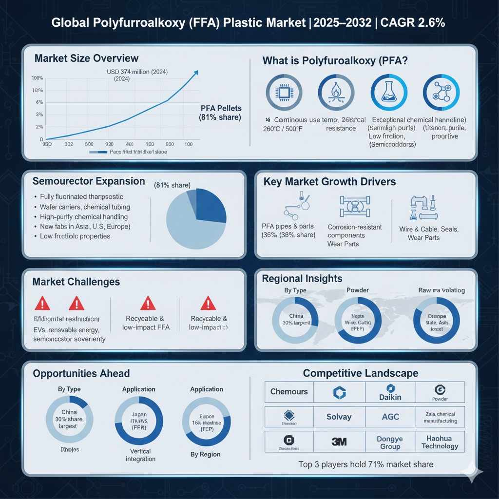
  • Global Polyfluoroalkoxy (PFA) Plastic Market to Reach USD 433 Million by 2032, Growing at 2.6% CAGR , Industry Forecast 2025–2032
    global Polyfluoroalkoxy (PFA) plastic market is set for steady growth, rising from USD 374 million in 2024 to an estimated USD 433 million by 2032 at a CAGR of 2.6%. PFA is a high-performance, fully fluorinated thermoplastic with exceptional chemical resistance, continuous-use temperatures up to 260 °C, outstanding dielectric properties, and ultra-high purity—making it indispensable in semiconductor manufacturing, chemical processing, electronics, and industrial applications. Demand is driven by accelerating semiconductor fabrication, increased need for corrosion-free chemical transfer equipment, and harsh-environment insulation. Although regulatory pressures and raw-material volatility remain challenges, innovation, recyclability efforts, and global industrial expansion offer promising long-term potential.
    Global Polyfluoroalkoxy (PFA) Plastic Market to Reach USD 433 Million by 2032, Growing at 2.6% CAGR , Industry Forecast 2025–2032 global Polyfluoroalkoxy (PFA) plastic market is set for steady growth, rising from USD 374 million in 2024 to an estimated USD 433 million by 2032 at a CAGR of 2.6%. PFA is a high-performance, fully fluorinated thermoplastic with exceptional chemical resistance, continuous-use temperatures up to 260 °C, outstanding dielectric properties, and ultra-high purity—making it indispensable in semiconductor manufacturing, chemical processing, electronics, and industrial applications. Demand is driven by accelerating semiconductor fabrication, increased need for corrosion-free chemical transfer equipment, and harsh-environment insulation. Although regulatory pressures and raw-material volatility remain challenges, innovation, recyclability efforts, and global industrial expansion offer promising long-term potential.
    0 留言 ·0 分享 ·243 瀏覽次數 ·0 評論
  • Global Antiseptic Products Market (2024–2032): Growth OutlGlobal Antiseptic Products Market, valued at USD 14.0 billion in 2024, is projected to reach USD 14.96 billion by 2032, growing at a CAGR of 1.0%. This market expansion is driven by rising hospital-acquired infections, increased hygiene awareness post-pandemic, and advancements in antiseptic formulations that enhance efficacy and reduce skin irritation. Antiseptic products—including alcohol-based solutions, povidone-iodine, chlorhexidine, and quaternary ammonium compounds—are widely used in surgical preparation, wound care, and hand hygiene. With strong demand across hospitals, clinics, and home-care settings, the market offers steady opportunities despite regulatory and environmental challenges.
    ok, Trends & Forecast at 1.0% CAGR
    Global Antiseptic Products Market (2024–2032): Growth OutlGlobal Antiseptic Products Market, valued at USD 14.0 billion in 2024, is projected to reach USD 14.96 billion by 2032, growing at a CAGR of 1.0%. This market expansion is driven by rising hospital-acquired infections, increased hygiene awareness post-pandemic, and advancements in antiseptic formulations that enhance efficacy and reduce skin irritation. Antiseptic products—including alcohol-based solutions, povidone-iodine, chlorhexidine, and quaternary ammonium compounds—are widely used in surgical preparation, wound care, and hand hygiene. With strong demand across hospitals, clinics, and home-care settings, the market offers steady opportunities despite regulatory and environmental challenges. ok, Trends & Forecast at 1.0% CAGR
    0 留言 ·0 分享 ·84 瀏覽次數 ·0 評論
  • Global Antiseptic Products Market (2024–2032): Growth Outlook, Trends & Forecast at 1.0% CAGR
    Global Antiseptic Products Market, valued at USD 14.0 billion in 2024, is projected to reach USD 14.96 billion by 2032, growing at a CAGR of 1.0%. This market expansion is driven by rising hospital-acquired infections, increased hygiene awareness post-pandemic, and advancements in antiseptic formulations that enhance efficacy and reduce skin irritation. Antiseptic products—including alcohol-based solutions, povidone-iodine, chlorhexidine, and quaternary ammonium compounds—are widely used in surgical preparation, wound care, and hand hygiene. With strong demand across hospitals, clinics, and home-care settings, the market offers steady opportunities despite regulatory and environmental challenges.
    Global Antiseptic Products Market (2024–2032): Growth Outlook, Trends & Forecast at 1.0% CAGR Global Antiseptic Products Market, valued at USD 14.0 billion in 2024, is projected to reach USD 14.96 billion by 2032, growing at a CAGR of 1.0%. This market expansion is driven by rising hospital-acquired infections, increased hygiene awareness post-pandemic, and advancements in antiseptic formulations that enhance efficacy and reduce skin irritation. Antiseptic products—including alcohol-based solutions, povidone-iodine, chlorhexidine, and quaternary ammonium compounds—are widely used in surgical preparation, wound care, and hand hygiene. With strong demand across hospitals, clinics, and home-care settings, the market offers steady opportunities despite regulatory and environmental challenges.
    0 留言 ·0 分享 ·84 瀏覽次數 ·0 評論
更多結果
MGBOX https://magicbox.mg