Doubly Bent Graphite Monochromators Gaining Strategic Importance in Synchrotron and Semiconductor
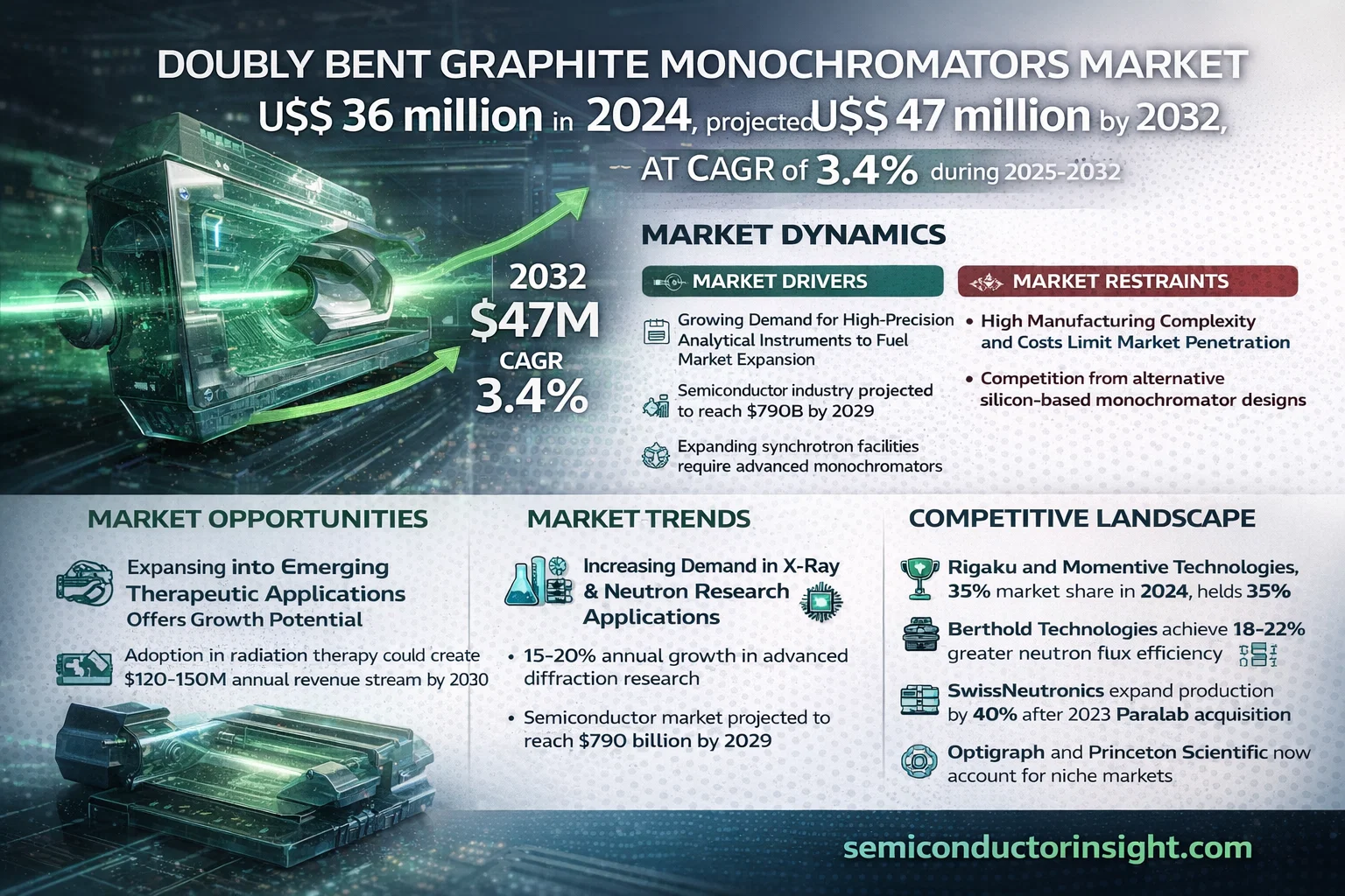
Global Doubly Bent Graphite Monochromators market is steadily gaining traction as advanced research facilities and semiconductor manufacturers demand higher wavelength precision and beam-focusing efficiency. Valued at USD 36 million in 2026, the market is projected to reach US$ 47 million by 2034, expanding at a CAGR of 3.4% during the forecast period 2026–2034.
Doubly bent graphite monochromators are high-precision optical components used to isolate specific wavelengths from polychromatic X-ray and neutron beams. Leveraging the unique properties of pyrolytic graphite, these components enable superior wavelength resolution and beam focusing compared to flat or singly bent monochromators, making them indispensable in materials science, physics, chemistry, and semiconductor inspection applications.
👉 Access the complete market intelligence, forecasts, and competitive benchmarking in the full report here:
Doubly Bent Graphite Monochromators Market Report
https://semiconductorinsight.com/report/doubly-bent-graphite-monochromators-market/
Rising Synchrotron Investments and Semiconductor Expansion Drive Market Momentum
The market’s growth trajectory is closely tied to global investments in synchrotron and neutron research infrastructure. Large-scale initiatives such as the EUR 1.8 billion European Spallation Source are accelerating demand for high-precision monochromators capable of handling intense radiation flux with consistent performance.
Simultaneously, the expanding semiconductor industry—projected to reach USD 790 billion by 2029—is creating additional demand for advanced X-ray diffraction and materials characterization tools. Leading manufacturers are responding with innovations focused on thermal stability, radiation resistance, and hybrid crystal configurations to meet next-generation research requirements.
Manufacturing Complexity and Alternative Technologies Create Competitive Pressure
Despite growing adoption, market penetration is constrained by high manufacturing complexity and production costs. Doubly bent graphite monochromators require ultra-high purity graphite (99.999%), sub-micron surface accuracy, and precision polishing processes that can account for 40–50% of total production costs. Long lead times—often exceeding 6–8 months for custom designs—further limit scalability.
At the same time, silicon-based monochromators are emerging as strong alternatives in the 5–20 keV energy range, offering improved thermal stability under high-flux conditions. While graphite monochromators maintain advantages in wavelength tunability and beam focusing, increasing adoption of silicon systems below 15 keV has resulted in gradual market share pressure.
Key Players Accelerating Innovation in Hybrid Monochromator Designs
Recent developments indicate a strong shift toward hybrid monochromators combining graphite with silicon or germanium crystals, delivering up to 30% improved thermal stability in high-flux environments. This trend is particularly evident in aerospace and semiconductor inspection applications, where precision tolerances are becoming increasingly stringent.
Key Market Participants Include:
- Rigaku Corporation (Japan)
- Momentive Technologies (U.S.)
- Berthold Technologies (Germany)
- SwissNeutronics AG (Switzerland)
- Optigraph GmbH (Germany)
- Princeton Scientific (U.S.)
- Spectral Instrument System (Italy)
- Gredmann China Limited (China)
- CAI Chemical Technologies (U.S.)
Segment Analysis Highlights Core Demand Centers
By Type
- Below 10 mm
- 10–20 mm
- Above 20 mm (leading due to higher X-ray efficiency)
By Application
- X-ray Diffraction (dominant segment)
- Neutron Diffractive
- Light Scattering
- Others
By End User
- Academic Research Institutions
- Industrial Laboratories
- Pharmaceutical Companies
- Government Research Facilities
North America and Europe Anchor Global Demand
North America leads adoption, driven by robust semiconductor R&D investment and advanced research facilities such as the Advanced Photon Source (APS) and SLAC National Accelerator Laboratory. In 2023 alone, U.S. semiconductor-related investments exceeded USD 52 billion, reinforcing demand for high-precision monochromators.
Europe follows closely, supported by strong photon science ecosystems in Germany and France and sustained funding through Horizon Europe (€95.5 billion, 2021–2027). However, the growing shift toward compact X-ray sources in medical and non-research applications may moderate long-term growth in certain segments.
Want to Review the Data Structure Before Purchase?
📄 Download a free sample of the report to explore segmentation, regional coverage, and analytical depth:
https://semiconductorinsight.com/download-sample-report/?product_id=103029
About Semiconductor Insight
Semiconductor Insight is a global intelligence platform delivering data-driven market insights, technology analysis, and competitive intelligence across the semiconductor and advanced electronics ecosystem. Our reports empower industry leaders, investors, policymakers, and OEMs with actionable insights into emerging technologies, high-growth markets, and strategic opportunities shaping the future of electronics.
🌐 https://semiconductorinsight.com/
🔗 LinkedIn: Follow Us
📞 International Support: +91 8087 99 2013
Categories
Read More
Buy Facebook Account with Marketplace in 2026Buy Facebook Account with Marketplace - USA, UK, CA, EU & AUSBuy Facebook Account with Marketplace: Simple GuideHow to Buy Facebook Account with MarketplaceTop 3 Sites to Buy Facebook Account with Marketplace3 Amazing Sites to Buy Facebook Account with MarketplaceWhere to Buy Facebook Account with MarketplaceHow to Buy Facebook Account...

If you want to buy USA Facebook accounts for your business, marketing, or personal needs, you’re not alone. Many people and companies buy USA Facebook accounts to save time, reach real US audiences, and get instant credibility. At ByteSMM, you can buy USA Facebook accounts—aged, verified, or in bulk—ready to use and fully secure. No hassle, no waiting, just results.Ready to...

If you’re here, chances are you’re looking to buy old Facebook accounts but want to make sure you’re making the right decision. Whether you’re a business owner, marketer, or someone who needs aged accounts for specific purposes, this guide will walk you through everything you need to know. At BestSMMExpert, we specialize in providing high-quality, secure, and reliable...