Photomask Blank (Binary, PSM, EUV) Market: Strategic Developments and Future Opportunities 2026-2034
The global Photomask Blank Market, encompassing binary masks, phase‑shifting masks (PSM) and extreme ultraviolet (EUV) blanks, continues to evolve as a cornerstone of the semiconductor manufacturing ecosystem. As chip designs become increasingly intricate and process nodes shrink below seven nanometers, the demand for high‑precision photomask blanks that can translate design intent into physical patterns with ever‑tighter tolerances is accelerating. The market is being driven by the convergence of several high‑technology trends, including the rollout of EUV lithography in leading foundries, the rise of artificial intelligence workloads, the expansion of high‑performance computingA and the global push toward 5G connectivity.
Photomask blanks serve as the foundational substrate upon which the most critical layers of an integrated circuit are projected. Their optical performance, defectivity control, and material stability directly influence yield, cycle time, and overall device cost. As semiconductor manufacturers pursue higher throughput and lower defect rates, the quality and availability of these blanks have become strategic differentiators for both equipment vendors and mask makers.
Download FREE Sample Report:
Photomask Blank (Binary, PSM, EUV) Market - View in Detailed Research Report
The rapid adoption of EUV lithography has reshaped the photomask blank landscape. EUV blanks, characterized by multilayer reflective coatings, are essential for patterning the most advanced nodes. Their production requires sophisticated deposition and inspection capabilities, leading to a concentration of capacity among a few highly specialized suppliers. At the same time, binary masks remain indispensable for mature nodes and cost‑sensitive applications, ensuring a balanced product mix that supports the entire semiconductor value chain.
Beyond the immediate lithography needs, photomask blanks are influencing broader industry dynamics. The emergence of heterogeneous integration, chiplet architectures, and advanced packaging solutions creates new mask‑related requirements, such as tighter overlay tolerances and specialized substrate materials. Moreover, the increasing emphasis on sustainability is prompting manufacturers to adopt greener processes, reduce waste, and improve the recyclability of mask materials.
COMPETITIVE LANDSCAPE
Key Industry Players
Photomask Blank Market Dominated by Leading Suppliers Amid Accelerated EUV Adoption
The photomask blank market is primarily led by a few dominant players including Hoya Corporation, AGC Inc., and S&S Tech Corporation, which together control around 85% of the global production capacity. These companies have established a robust presence through extensive technological capabilities and capacity expansion, addressing a broad range of semiconductor lithography needs from binary and phase‑shifting masks (PSM) to advanced extreme ultraviolet (EUV) blanks. The market structure reflects a high degree of concentration, particularly as demand surges for sub‑7nm node production and High‑NA EUV technologies, with leading foundries such as TSMC and Samsung driving significant growth through their advanced chip manufacturing requirements.
Besides the market leaders, several niche yet significant players contribute specialized photomask blank solutions tailored to specific semiconductor processes or regional demands. Companies like Mitsui Chemicals, Shin‑Etsu Chemical, and HOYA ALPHA Plastics provide competitive offerings, often focusing on innovation within binary and PSM segments. Moreover, emerging suppliers such as Corning Incorporated and Fukuda Chemicals are investing in next‑generation blank technologies to keep pace with evolving industry standards. This diverse competitive environment supports ongoing advancements in semiconductor lithography driven by AI, high‑performance computing, and 5G application demands.
List of Key Photomask Blank Companies Profiled
-
Hoya Corporation
-
S&S Tech Corporation
-
Shin-Etsu Chemical
-
Fukuda Chemicals
-
Komatsu Ltd.
-
Seiko Epson Corporation
-
Tantec Ltd.
-
Fujifilm Holdings Corporation
-
Tokuyama Corporation
Segment Analysis:
| Segment Category | Sub-Segments | Key Insights |
| By Type |
|
Extreme Ultraviolet (EUV) Mask Blanks are rapidly gaining prominence due to their critical role in next‑generation semiconductor nodes, supporting sub‑7nm technologies. Their advanced multilayer reflective coatings are indispensable for high‑resolution chip fabrication.
|
| By Application |
|
Semiconductor Manufacturing remains the primary application area where advancements in photomask blanks directly contribute to improvements in chip resolution and functionality.
|
| By End User |
|
Foundries dominate demand due to their focus on cutting‑edge fabrication nodes, especially the push towards 3nm and smaller technologies requiring EUV mask blanks.
|
| By Lithography Technology |
|
Extreme Ultraviolet (EUV) lithography is a key driver for demand in advanced photomask blanks, enabling critical resolution enhancements.
|
| By Supplier Type |
|
Specialized Photomask Manufacturers such as industry leaders provide critical technology and production capacity to meet advanced blank specifications.
|
Regional Analysis: Global Photomask Blank (Binary, PSM, EUV) Market
The Asia‑Pacific region benefits from continuous innovation in photomask blank design, particularly enhancing EUV blank defectivity and binary blank uniformity. Collaboration between equipment suppliers and semiconductor fabs accelerates technology adoption, supporting the evolution of complex patterning techniques.
Strong vertical integration and supply chain coordination characterize Asia‑Pacific’s photomask blank market. Local suppliers manage raw material sourcing and finishing processes to reduce lead times and improve responsiveness to fab requirements.
Increasing semiconductor wafer fabrication capacity expansion driven by consumer electronics and automotive industries directly boosts photomask blank consumption. Strategic government initiatives on semiconductor autonomy also underpin sustained growth.
Despite notable advances, managing complex defect inspection requirements and cost pressures remains a challenge. However, the rising demand for EUV photomask blanks presents ample opportunity for innovation and market differentiation.
North America
North America maintains a significant role in the Photomask Blank (Binary, PSM, EUV) Market through its concentration of semiconductor design houses and cutting‑edge fab operations. The region excels in developing advanced mask‑making technologies, focusing on improving defect control and mask durability to address increasingly smaller process nodes. Collaboration among leading equipment manufacturers, mask shops, and fabs fosters innovation. Moreover, initiatives to strengthen domestic semiconductor manufacturing contribute to sustained demand, enhancing North America’s strategic importance in the photomask blank supply chain.
Europe
Europe’s presence in the Photomask Blank (Binary, PSM, EUV) Market is driven by specialised research institutions and companies developing niche photomask products, particularly for PSM and binary masking solutions. The region emphasizes sustainability and precision manufacturing, complementing its focus on automotive semiconductors and industrial electronics. Collaborative projects under the European Union’s semiconductor initiatives promote advanced photomask blank technologies, although the overall market size remains optimistic but comparatively moderate.
South America
South America exhibits nascent activity in the photomask blank arena with growing interest in semiconductor component assembly and testing. Although direct manufacturing of photomask blanks remains limited, the market benefits indirectly from increasing fab outsourcing and demand for high‑quality mask blanks related to regional electronics manufacturing growth. Strategic partnerships and investments could accelerate the region’s photomask blank capabilities in coming years.
Middle East & Africa
The Middle East & Africa market for photomask blanks is in early development stages, with emerging investments in semiconductor fabrication and advanced manufacturing clusters. Demand is currently limited but shows potential linked to regional diversification into high‑tech industries. Efforts focusing on technology transfers and infrastructure development may gradually strengthen the market position in this region, particularly for next‑generation EUV photomask blanks.
Get Full Report Here:
Photomask Blank (Binary, PSM, EUV) Market, Trends, Business Strategies 2026-2034 - View in Detailed Research Report
About Semiconductor Insight
Semiconductor Insight is a leading provider of market intelligence and strategic consulting for the global semiconductor and high‑technology industries. Our in‑depth reports and analysis offer actionable insights to help businesses navigate complex market dynamics, identify growth opportunities, and make informed decisions. We are committed to delivering high‑quality, data‑driven research to our clients worldwide.
Click Here to Explore More Insightful Result
https://semiconductorinsight.com/blog/tag/acoustic-wave-technology-biosensors-market/
https://semiconductorinsight.com/blog/tag/wireless-bluetooth-speaker-chips-market/
https://semiconductorinsight.com/blog/tag/electrically-erasable-rom-market-growth-2/
https://semiconductorinsight.com/blog/tag/regenerative-battery-pack-test-systems-market-trends/
https://semiconductorinsight.com/blog/tag/two-way-tower-mounted-amplifiers-market-trends/
🌐 Website: https://semiconductorinsight.com/
📞 International: +91 8087 99 2013
🔗 LinkedIn: Follow Us
Categories
Read More
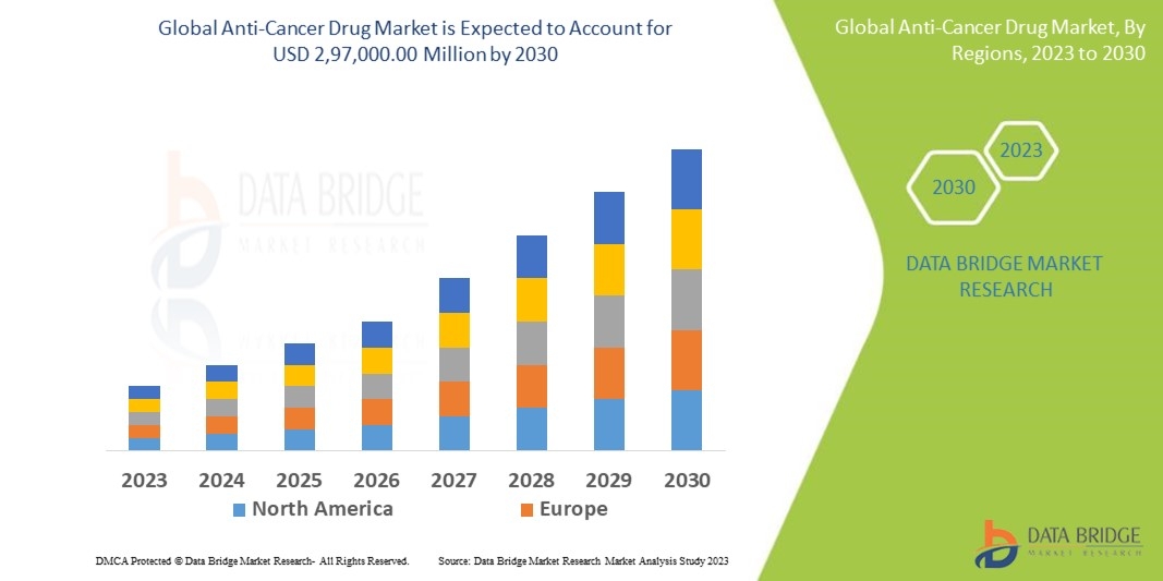
According to the latest report published by Data Bridge Market Research, the Anti-Cancer Drug Market The global anti-cancer drug market which was USD 1,20,000.00 million in 2022, would rocket up to USD 2,97,000.00 million by 2030, and is expected to undergo a CAGR of 12.0% during the forecast period. This indicates the market value. “Oral” dominates the “Route of...
Gmail Account Security, Management, Productivity & Business Guide 2026 Introduction 🌟🌟🌟🌟🌟🌟🌟🌟🌟🌟🌟🌟🌟🌟🌟🌟🌟🌟🌟🌍 24/7 Customer Support Available💬 Telegram:@usadigitalhub📧 Email:usadigitalhubsell@gmail.com🟣 Discord Community:usadigitalhub🌐 Visit Our Website:👉https://usadigitalhub.com/product/buy-old-gmail-accounts/🌟🌟🌟🌟🌟🌟🌟🌟🌟🌟🌟🌟🌟🌟🌟🌟🌟🌟🌟 Email remains one of the most important communication tools in the...