Wafer-level Test and Burn-in (WLTBI) Market to Reach USD 800 Million by 2034 at 7.3% CAGR
Global Wafer-level Test and Burn-in (WLTBI) Market size was valued at USD 394.6 million in 2024 and is projected to reach USD 800 million by 2034, at a CAGR of 7.3% during the forecast period 2026-2034. Strong growth trajectory reflects advanced 2.5D/3D packaging proliferation and automotive functional safety mandates.
Wafer-level Test and Burn-in encompasses full-field electrical characterization and accelerated stress screening of 300mm wafers at -40°C to 150°C, identifying infant mortality defects prior to costly singulation and packaging flows. These systems deliver 10,000+ wafer/month throughput with sub-1°C thermal uniformity across HBM4 stacks, CoWoS-R chiplet clusters, and SiP modules, achieving 15-20% yield uplift versus package-level test while slashing handling costs 40%.
👉 Access the complete industry analysis and demand forecasts here: https://semiconductorinsight.com/report/global-wafer-level-test-and-burn-in-wltbi-market/
Market Definition and Dynamics
WLTBI Market supplies full-wafer contactors and thermal chambers for parametric DC/functional test plus high-temperature operating life (HTOL) acceleration before dicing, propelled by chiplet decomposition requiring known-good-die (KGD) validation and AEC-Q100 Grade 0 automotive qualification.
Equipment evolution features MEMS pogo arrays achieving 99.9% first-contact yield on 10µm pads, liquid nitrogen shrouds enabling -55°C to 175°C ramps in <5 minutes, and ML-driven pattern recognition flagging 85% of systematic defects pre-packaging.
Market Drivers
- Advanced packaging capacity scaling to 4M 300mm-equivalent wafers/month for CoWoS/InFO/HBM driving 25% annual WLTBI spend growth.
- Automotive AEC-Q100 Grade 0 (-40°C/175°C, 1,000hr HTOL) qualification consuming 2x burn-in hours versus consumer silicon.
- OSAT 300mm FOWLP lines requiring KGD sort prior to redistribution layer (RDL) processing, avoiding 30% rework scrap.
- Five-foundry model expansion (TSMC/GlobalFoundries/UMC/Samsung/SMIC) mandating test harmonization across regional nodes.
Market Restraints
- USD 5M+ system capex plus USD 2M cleanroom modification creating 3-year minimum ROI threshold for mid-tier OSATs.
- 300mm full-field thermal gradient >±2°C causing 3-5% parametric outliers in HBM/DRAM density-sensitive applications.
- 12-18 month lead times for custom probe cards and chamber components delaying capacity ramps during demand spikes.
Market Opportunities
- 450mm pioneer lines requiring next-gen full-wafer contactors for Intel's 14A/Intel 10 process technology pilots.
- Silicon photonics test consuming 5x touch-downs per wafer for grating coupler alignment and modulator BIST.
- CFET (Complementary FET) cell test development for 1.4nm-class gate-all-around requiring cryogenic WLTBI flows.
- Defense/aerospace rad-hard qualification creating 10-year lifecycle revenue streams at 3x commercial pricing.
Competitive Landscape
Aehr Test Systems commands 28% leadership through FOX-XP full-wafer IP, PentaMaster captures 18% Asian volume via multi-site parallelization, while regional specialists erode pricing through automotive niche focus.
List of Key Wafer-level Test and Burn-in Companies
- Aehr Test Systems (U.S.)
- PentaMaster (South Korea)
- Delta V Systems (Germany)
- Electron Test (U.S.)
- Advantest Corporation (Japan)
- Teradyne (U.S.)
- FormFactor, Inc. (U.S.)
- Tokyo Electron Limited (Japan)
- Cohu, Inc. (U.S.)
Segment Analysis By Type
Full wafer systems capture 65% revenue through mass production efficiency, multi-wafer parallelization growing fastest at 9.2% CAGR for HBM qualification, while single-wafer platforms serve low-volume power/RF device characterization.
By Application
OSATs drive 55% volume growth through FOWLP/HBM test outsourcing, IDMs maintain 45% premium revenue for proprietary automotive/AI silicon validation.
Regional Insights
Asia-Pacific dominates 68% capacity via TSMC/ASE/Hynix 300mm lines, North America captures 20% value through Intel/GlobalFoundries advanced packaging R&D, Europe leads automotive AEC-Q100 qualification (12%), while South America/MEA emerge via regional OSAT buildout.
👉 Access the complete industry analysis and demand forecasts here:
https://semiconductorinsight.com/report/global-wafer-level-test-and-burn-in-wltbi-market/
📄 Download a free sample to explore segment dynamics and competitive positioning:
https://semiconductorinsight.com/download-sample-report/?product_id=95848
About Semiconductor Insight
Semiconductor Insight is a global intelligence platform delivering data-driven market insights, technology analysis, and competitive intelligence across the semiconductor and advanced electronics ecosystem. Our reports support OEMs, investors, policymakers, and industry leaders in identifying high-growth markets and strategic opportunities shaping the future of electronics.
🌐 https://semiconductorinsight.com
🔗 LinkedIn:Follow Us
📞 International Support: +91 8087 99 2013
Categories
Read More
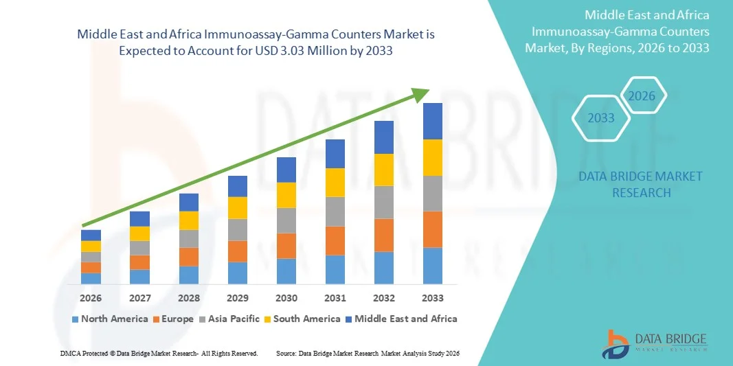
Executive Summary Middle East and Africa Immunoassay-Gamma Counters Market Size and Share Forecast The Middle East and Africa immunoassay-gamma counters market size was valued at USD 2.23 million in 2025 and is expected to reach USD 3.03 million by 2033, at a CAGR of 3.9% during the forecast period Middle East and Africa Immunoassay-Gamma Counters Market...
Buy Verified Revolut Business Account – A Smart Financial Solution for Modern Businesses Contact Info ✅WhatsApp: +1 (781) 281-8745 ✅Telegram: @RealShopUSA ✅Skype: RealShopUSA ✅Email: support@realshopusa.com Visit Our Shop ✅https://realshopusa.com/product/buy-verified-revolut-account/ In today’s fast-paced digital...