Wafer Bonding Equipment Market to Reach USD 620 Million by 2034 Driven by 3D IC and MEMS
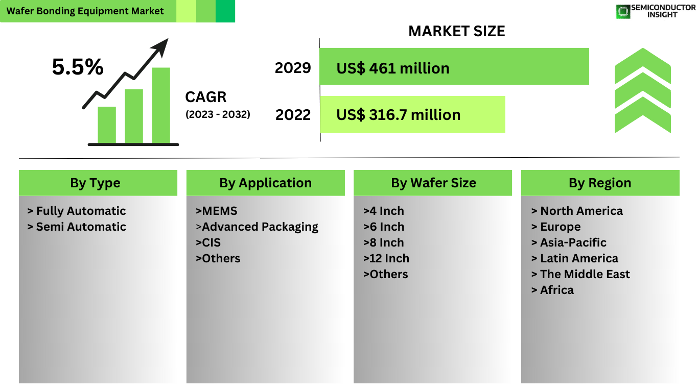
global Wafer Bonding Equipment Market was valued at USD 317 million in 2024 and is projected to reach USD 620 million by 2034, at a CAGR of 7.1% during the forecast period 2026-2034. Consistent growth reflects rising complexity in advanced packaging and heterogenous integration across semiconductors.
Wafer bonding equipment comprises precision semiconductor processing tools that permanently join multiple wafers or substrates through techniques including direct fusion, hybrid, adhesive, anodic, and thermal compression bonding. These systems feature aligned vacuum chambers, plasma activation modules, high-force presses capable of 100kN+ pressure, and in-situ metrology for sub-100nm overlay accuracy, operating across 200mm-450mm wafer formats under ultra-clean conditions👉 Access the complete industry analysis and demand forecasts here: https://semiconductorinsight.com/report/wafer-bonding-equipment-market/
Market Definition and Dynamics
The Wafer Bonding Equipment Market includes capital equipment for wafer-level permanent and temporary bonding in semiconductor fabs, fueled by macro shifts toward chiplet-based architectures, HBM4+ memory stacking, and co-packaged optics for AI datacenters. Core forces encompass node shrinks below 2nm demanding thin-wafer handling under 50µm, CFET/3D transistor integration requiring precise layer stacking, and photonics convergence needing low-loss SiN-Si bonding.
Market Drivers
- Surge in 3D IC/heterogenous integration for AI/HPC, with HBM stacking projected to consume 30%+ of advanced bonding capacity by 2028.
- MEMS proliferation in automotive/consumer IoT, where cavity-sealed gyroscopes/accelerometers require anodic/adhesive bonding for >10-year hermeticity.
- Advanced packaging roadmaps (CoWoS, Foveros) mandating temporary bonding/debonding for ultra-thin TSV processing at <30µm handles.
- Power semiconductor verticalization via SiC/GaN-on-Si bonding, enabling 1200V+ modules with 40% lower Rdson.
Market Restraints
- High capex intensity exceeding USD 10M per fully automated tool, limiting adoption to top-tier fabs with 300mm+ lines.
- Process complexity in hybrid bonding demanding <1nm surface roughness and 0.5° planarity, extending qual cycles to 12+ months.
- Throughput bottlenecks in R&D tools versus production systems, constraining scale-up for emerging nodes.
Market Opportunities
- Chiplet ecosystems expanding hybrid bonding for multi-die systems, targeting USD 50B advanced packaging market by 2030.
- Photonics/silicon photonics requiring low-loss fusion for SiN waveguides and grating couplers in datacom transceivers.
- CFET/GAA transistor stacking via direct bonding, unlocking 20%+ density gains at 1nm-class nodes.
- Regional fab builds in India/US/Europe creating localized demand amid supply chain diversification.
Competitive Landscape
Leading OEMs command 70%+ share through fully automated platforms with integrated metrology and AI-driven alignment. EV Group dominates hybrid bonding IP, while SUSS excels in temporary bonding for MEMS. Tokyo Electron leverages etch/bond cluster tools for high-volume.
List of Key Wafer Bonding Equipment Companies
- EV Group (Austria)
- SUSS MicroTec (Germany)
- Tokyo Electron (Japan)
- Applied Microengineering (U.S.)
- Nidec Machinetool (Japan)
- Ayumi Industry (Japan)
- Shanghai Micro Electronics (China)
- U-Precision Tech (Taiwan)
- Hutem (Taiwan)
- Canon (Japan)
- Bondtech (U.S.)
- TAZMO (Japan)
- TOK (Japan)
- Kulicke & Soffa (U.S.)
Segment Analysis By Type
- Fully Automatic
- Semi Automatic
By Application
- MEMS
- Advanced Packaging
- CIS
- Others
By Wafer Size
- 4 Inch
- 6 Inch
- 8 Inch
- 12 Inch
- Others
Regional Insights
Asia-Pacific maintains 60%+ dominance via Japan/China/Taiwan fabs ramping HBM/3D NAND, North America grows via Intel/TSMC US plants focusing hybrid bonding, Europe strong in MEMS/RF via Infineon/SOITEC, South America/MEA emerge in power device assembly amid EV localization.
👉 Access the complete industry analysis and demand forecasts here:
https://semiconductorinsight.com/report/wafer-bonding-equipment-market/
📄 Download a free sample to explore segment dynamics and competitive positioning:
https://semiconductorinsight.com/download-sample-report/?product_id=3350
About Semiconductor Insight
Semiconductor Insight is a global intelligence platform delivering data-driven market insights, technology analysis, and competitive intelligence across the semiconductor and advanced electronics ecosystem. Our reports support OEMs, investors, policymakers, and industry leaders in identifying high-growth markets and strategic opportunities shaping the future of electronics.
🌐 https://semiconductorinsight.com
🔗 LinkedIn:Follow Us
📞 International Support: +91 8087 99 2013
Categories
Read More
Buy Old Gmail Accounts Buy Are you exploring the digital landscape for a strategic advantage? If so, consider the potential of old Gmail accounts. They may seem like relics from a bygone era, yet they offer unique benefits that modern accounts simply can’t match. As businesses strive to build trust and credibility online, many are turning to these aged accounts as an essential tool in...

If you want to buy Trustpilot reviews, you’re in the right place. At EverSMM, we make it easy, safe, and quick to buy Trustpilot reviews—whether you need positive, negative, or custom packages. No complicated steps, no confusing jargon—just a straightforward solution for anyone who wants to improve their online reputation and build trust with real customers.Ready to get...

If you’re looking to buy Facebook accounts bulk, you’re in the right place. Whether you’re a business owner, marketer, or someone managing multiple campaigns, buying Facebook accounts in bulk can save you time, effort, and money. At BestSMMExpert, we specialize in providing high-quality, secure, and reliable Facebook accounts in bulk to help you scale your operations...

Executive Summary Surgical Snare Market : Data Bridge Market Research analyses that the surgical Snare market which was USD 1,210.11 million in 2022, would rocket up to USD 2,132.58 million by 2030, and is expected to undergo a CAGR of 11.6% during the forecast period. The high quality Surgical Snare Market report not only takes into consideration all the market drivers and...
If you want to buy negative Trustpilot reviews, you’re in the right place. At ByteSMM, we make it easy, safe, and quick to buy negative Trustpilot reviews. Whether you need just one, a handful, or a steady stream. No complicated steps, no confusing jargon, just a simple solution for anyone who wants to manage online reputations, balance review profiles, or even keep the competition...